Research
Scanning Photo-induced Impedance Microscopy (SPIM)
| Principal investigator: | Steffi KRAUSE |
| Co-investigator(s): | W. Moritz (Humboldt University Berlin) |
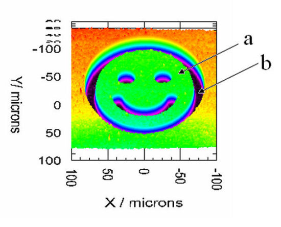
 AC impedance spectroscopy is a powerful technique for the investigation of electrochemical interfaces and thin and thick films. It provides information about electrochemical reactions, coverage, conductivity and pore formation. However, a major drawback is that the information obtained always represents the properties averaged across the whole sample area. A novel technique, Scanning Photo-Induced Impedance Microscopy (SPIM), that allows the use of impedance measurements for the imaging of film properties, has been developed.