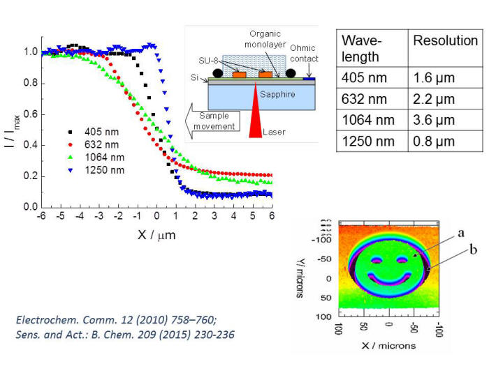
High resolution LAPS and SPIM
Highlights of this research are:
- the achievement of submicron resolution,
- the increase in the sensitivity of SPIM using organic, self-assembled monolayers as insulators and
- quantitative impedance imaging of polyelectrolyte microcapsules with high resolution.
High resolution was achieved by using silicon-on-sapphire as the semiconductor substrate and by using a two-photon effect in silicon.
Organic monolayers were introduced as the insulator to improve the sensitivity and accuracy of SPIM and LAPS.
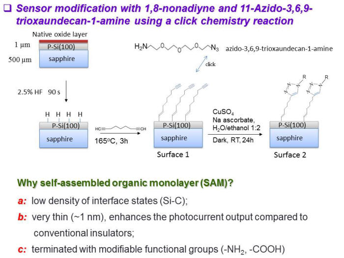
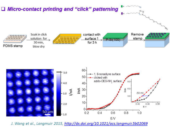
Organic monolayers obtained by reacting 1,8-nonadiyne with the H-terminated silicon surface can easily be modified by copper catalysed click chemistry. The method was adapted for microcontact printing for patterning surfaces with functional groups. Photocurrent images of the patterned samples clearly show an increase in the photocurrent due to the positive surface charge of the -NH2 modified surface
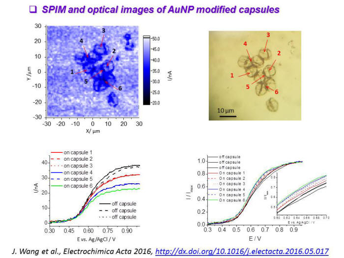
Polyelectrolyte microcapsules modified with gold nanoparticles were produced using a layer-by-layer technique.
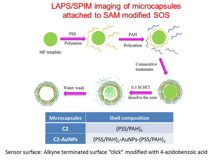
The gold-modified microcapsules were deposited and collapsed on the sensor surface. SPIM images show the local variation in impedance in great detail.