News
Queen Mary researchers develop non-distructive single-crystal perovskite surface nanopatterning technologies
25 September 2020

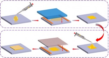
Patterning process

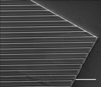
Patterned thin film
Single-crystalline perovskites are widely regarded as the future semiconductor materials and will be the next big wave in optoelectronics. To manufacture high-quality single-crystal perovskite optoelectronics, non-destructive surface nanopatterning technologies are required. Conventional photolithography-based nanopatterning methods cannot be used due to perovskite’s sensitivity to high temperature and solvents.
Researchers at Queen Mary University of London invented a cost-effective simple method for the epitaxial growth of high-quality nanopatterns on single-crystal perovskite thin-film surface, which is potentially suitable for mass producing perovskite optoelectronic devices. By using their technology, nanopatterns with any desirable shape and geometry at a resolution down to tens of nanometres on single-crystal perovskite thin films were achieved and were proven to be the same single-crystal structure.
This technology may open new possibilities for the development of novel nanometer-scale hybrid perovskite on-chip optoelectronic devices.
https://pubs.acs.org/doi/abs/10.1021/acsnano.9b08553
| People: | Lei SU Haixue YAN Martin KNIGHT Colin HUMPHREYS |
Updated by: Lei Su


